You are hereIntegrated FPGA support with OpenComRTOS Designer
Integrated FPGA support with OpenComRTOS Designer
Altreonic announces integrated FPGA support for its multicore/manycore capable OpenComRTOS Designer on Microsemi’s SmartFusion-II.
 Advanced chip technology has in the last decade reached a level of integration whereby complete systems can now be made available in a single package. Such Systems On a Chip (SoC) contains often multiple types of processor cores, each specialized for their function, but also smart I/O blocks, on chip networks, caches and program as well as data memory. Recent chips also add FPGA logic blocks.
Since 2005 Altreonic has developed a formally developed runtime system and development environment called OpenComRTOS Designer. Formally developed, it has a typical code size of 5 to 10 KB and supports systems in a fully scalable way. It transparently supports systems with heterogeneous processing nodes as well as heterogeneous communication mechanisms. This makes it suitable for networked, distributed systems as well as for on-chip many/multicore SoC. Board Support packages have been developed for example for TI’s C6678 8-core multi-DSP, Intel’s 48-core SCC as well as for multicore ARM and PPC systems, often replacing traditional memory hungry POSIX-style RTOS.
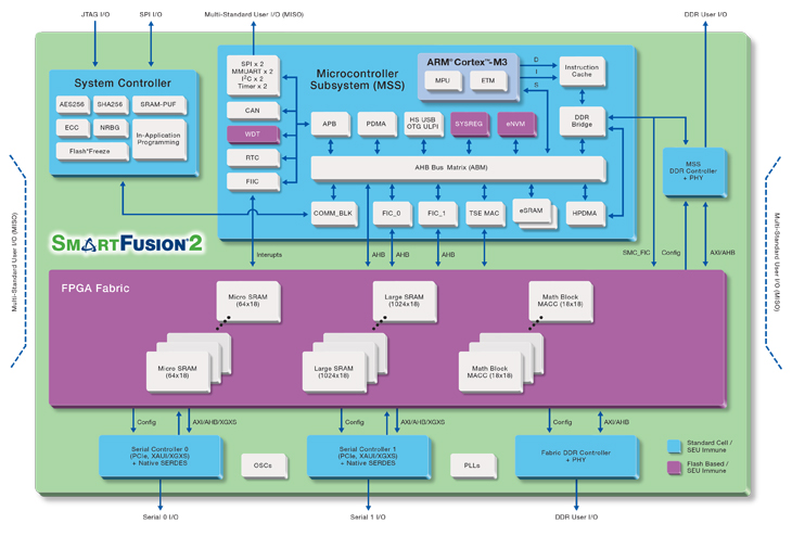
Today, Altreonic announces integrated FPGA support, demonstrated on Microsemi’s SmartFusion-II. On this chip the user finds a 166 MHz ARM Cortex M3, DMA, I/O blocks and memory as well as a flash programmable FPGA logic. Traditional approaches will treat the FPGA as a co-processing block that is explicitly accessed using dedicated software running on the ARM. In OpenComRTOS tasks synchronise and communicate using so-called intermediate “hub entities” that fully decouple tasks allowing them to be anywhere in the network whereby OpenComRTOS takes cares of the inter-node communication.
To support the FPGA logic, a generic service was developed whereby tasks interface through a so-called FPGA-hub. The example shows how the developer can add application specific services to the OpenComRTOS kernel (without changing the kernel code itself as most of the additions are described in an external metamodel. The benefits are multiple:
- The FPGA can be accessed from any task, anywhere in the system.
- The FPGA blocks can easily be shared between several tasks.
- The application is practically identical whether using the FPGA block or calling an equivalent software implemented function.
- The application software can see a significant performance improvement (typically a factor 10 to 30 depending on the function).
Key performance data for OpenComRTOS on SmartFusion-II (166 MHz) using the PDMA for the data transfer form main memory to the FPGA and back:
1.Code size of the RTOS kernel (all services): 4708 bytes (excl. the ARM start-up code).
2.Interrupt latency (using a standardized test set-up, program cache enabled):
- IRQ to ISR latency: 366 to 1296 (worst case), typically 390 nanoseconds
- IRQ to Task latency: 8 to 22 (worst case), typically 10 microseconds.
3.Semaphore loop (4 kernel services and 4 semaphore operations: 18.56 microseconds. Program cache enabled.
4.FPGA benchmark for a 1K FFT, radix-2, fixed point. The test set-up reads the data from the same memory location and writes back the results to memory. Program cache disabled.
- Application calling the FFT in software: 8531 microseconds.
- Application calling the FFT in the FPGA: 218 microseconds.
- FPGA/CPU speed-up: 39.16
5.FPGA benchmark for a 1K FFT, radix-2, fixed point. The test set-up reads the data from the same memory location and writes back the results to memory. Program cache enabled.
- Application calling the FFT in software: 2304 microseconds.
- Application calling the FFT in the FPGA: 188 microseconds
- FPGA/CPU speed up: 12.26
6.FPGA benchmark for a 4K FFT, radix-2, fixed point. The test set-up reads the data from the same memory location and writes back the results to memory. Program cache enabled.
- Application calling the FFT in software: 10866 microseconds.
- Application calling the FFT in the FPGA: 731 microseconds.
- FPGA/CPU speed up: 14.87
More information can be found at: www.altreonic.com
Share |
More information can be found at: www.altreonic.com
- Printer-friendly version
- Login to post comments